RAD DATA COMMUNICATIONS
UCI/HS
| Card Type | Modem eliminator, interface converter, serial elastic buffer (synchronous) |
| Chipset | Unidentified |
| Maximum Data Rate | 2.048Mbps |
| Data Bus | Serial |

CONNECTIONS |
|||
Function |
Label |
Function |
Label |
| Header for serial port module 1 | J1 |
AC power in | J3 |
| Header for serial port module 2 | J2 |
||
USER CONFIGURABLE SETTINGS |
|||
Setting |
Label |
Position |
|
| » | Clock source is internal | JP3 |
Pins 3 & 4 closed |
| Clock source is serial port 1 transmit clock | JP3 |
Pins 1 & 2 closed |
|
| » | DCD of serial port 1 forced high | JP4 |
Pins 1 & 2 closed |
| DCD of serial port 1 controlled by RTS of serial port 2 | JP4 |
Pins 3 & 4 closed |
|
| » | DCD of serial port 2 forced high | JP5 |
Pins 1 & 2 closed |
| DCD of serial port 2 controlled by RTS of serial port 1 | JP5 |
Pins 3 & 4 closed |
|
| » | Signal ground not connected to chassis ground | JP7 |
Pins 1 & 2 closed |
| Signal ground connected to chassis ground | JP7 |
Pins 2 & 3 closed |
|
SERIAL PORT 1 RTS TO CTS DELAY |
||||
Setting |
JP2/A |
JP2/B |
JP2/C |
|
| » | 0 mS |
Open |
Open |
Closed |
6 mS |
Open |
Closed |
Open |
|
51 mS |
Closed |
Open |
Open |
|
SERIAL PORT 2 RTS TO CTS DELAY |
||||
Setting |
JP1/A |
JP1/B |
JP1/C |
|
| » | 0 mS |
Open |
Open |
Closed |
6 mS |
Open |
Closed |
Open |
|
51 mS |
Closed |
Open |
Open |
|
MODE SELECTION |
||||
Setting |
JP6/A |
JP6/B |
JP6/C |
|
| » | Modem eliminator |
Open |
Open |
Closed |
Interface converter |
Open |
Closed |
Open |
|
Elastic buffer |
Closed |
Open |
Open |
|
SERIAL PORT SPEED SELECTION |
|
Setting |
SW1 |
48Kbps |
Position 8 |
56Kbps |
Position 9 |
64Kbps |
Position A |
112Kbps |
Position B |
128Kbps |
Position 7 |
256Kbps |
Position 6 |
384Kbps |
Position 5 |
512Kbps |
Position 4 |
768Kbps |
Position 3 |
1.024Kbps |
Position 2 |
1.544Kbps |
Position 1 |
2.048Mbps |
Position 0 |
DIAGNOSTIC LED(S) |
|||
LED |
Color |
Status |
Condition |
LED1 |
Unidentified |
On |
Power is on |
LED1 |
Unidentified |
Off |
Power is off |
LED2 |
Unidentified |
On |
Serial port 1 is transmitting data |
LED2 |
Unidentified |
Off |
Serial port 1 is not transmitting data |
LED3 |
Unidentified |
On |
Serial port 1 is receiving data |
LED3 |
Unidentified |
Off |
Serial port 1 is not receiving data |
LED4 |
Unidentified |
On |
Serial port 2 is transmitting data |
LED4 |
Unidentified |
Off |
Serial port 2 is not transmitting data |
LED5 |
Unidentified |
On |
Serial port 2 is receiving data |
LED5 |
Unidentified |
Off |
Serial port 2 is not receiving data |
LED6 |
Unidentified |
On |
Device is in interface converter mode |
LED6 |
Unidentified |
Off |
Device is not in interface converter mode |
LED7 |
Unidentified |
On |
Device is in elastic buffer mode |
LED7 |
Unidentified |
Off |
Device is not in elastic buffer mode |
LED8 |
Unidentified |
On |
Device is in modem eliminator mode |
LED8 |
Unidentified |
Off |
Device is not in modem eliminator mode |
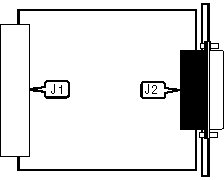
UCI (G.703 SERIAL MODULE)
| Card Type | Serial |
| Chipset | Unidentified |
| I/O Options | Serial port |

CONNECTIONS |
|||
Function |
Label |
Function |
Label |
| Header to main board J1 or J2 | J1 |
G.703 serial port via DB-15 connector | J2 |
USER CONFIGURABLE SETTINGS |
|||
Setting |
Label |
Position |
|
| » | Line speed is 64Kbps | JP1 |
Unidentified |
| Line speed is 128Kbps | JP1 |
Unidentified |
|
| » | Card will use external clock source | JP2 |
Unidentified |
| Card will use internal clock source | JP2 |
Unidentified |
|
| Note:The exact location and configuration of these jumpers is unidentified. | |||
| Card Type | Serial |
| Chipset | Unidentified |
| I/O Options | Serial port |

CONNECTIONS |
|||
Function |
Label |
Function |
Label |
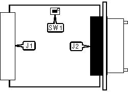
| Header to main board J1 or J2 | J1 |
V.35 serial port | J2 |
USER CONFIGURABLE SETTINGS |
||
Setting |
Label |
Position |
| Serial port is DCE | SW1 |
Off |
| Serial port is DTE | SW1 |
On |
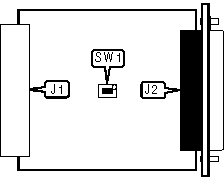
UCI/HS (V.36 SERIAL MODULE)
| Card Type | Serial |
| Chipset | Unidentified |
| I/O Options | Serial port |

CONNECTIONS |
|||
Function |
Label |
Function |
Label |
| Header to main board J1 or J2 | J1 |
V.36 serial port via DB-37 connector | J2 |
USER CONFIGURABLE SETTINGS |
||
Setting |
Label |
Position |
| Serial port is DCE | SW1 |
Off |
| Serial port is DTE | SW1 |
On |
| Card Type | Serial |
| Chipset | Unidentified |
| I/O Options | Serial port |

CONNECTIONS |
|||
Function |
Label |
Function |
Label |
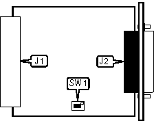
| Header to main board J1 or J2 | J1 |
X.21 serial port via DB-15 connector | J2 |
USER CONFIGURABLE SETTINGS |
||
Setting |
Label |
Position |
| Serial port is DCE | SW1 |
Off |
| Serial port is DTE | SW1 |
On |
UCI/HS (V.24 SERIAL MODULE)
| Card Type | Serial |
| Chipset | Unidentified |
| I/O Options | Serial port |

CONNECTIONS |
|||
Function |
Label |
Function |
Label |
| Header to main board J1 or J2 | J1 |
V.24 serial port via DB-25 connector | J2 |
USER CONFIGURABLE SETTINGS |
||
Setting |
Label |
Position |
| Serial port is DCE | SW1 |
Off |
| Serial port is DTE | SW1 |
On |
| Card Type | T1/E1 CSU/DSU |
| Chipset | Unidentified |
| T1/E1 Transfer Rate | 1.544Mbps/2.048Mbps |
| T1/E1 Protocol | Unidentified |
| Frame Type | Unidentified |

CONNECTIONS |
|||
Function |
Label |
Function |
Label |
| Header to main board J1 or J2 | J1 |
T1/E1 interface | J3 |
| T1/E1 interface | J2 |
||
TRANSMIT CLOCK SOURCE |
|||
Setting |
JP1/A |
JP1/B |
JP1/C |
Internal |
Closed |
Open |
Open |
External |
Open |
Closed |
Open |
Loopback |
Open |
Open |
Closed |
MISCELLANEOUS TECHNICAL NOTE |
| The T1/E1 interface module may only be used when the other installed module is a V.35, X.21, or RS-530 interface. |