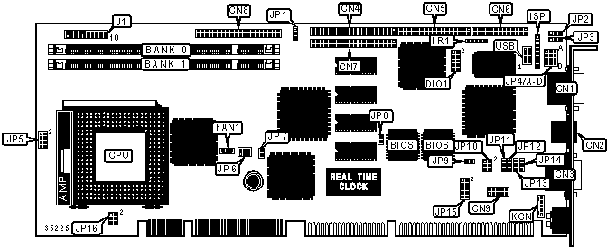
LANNER ELECTRONICS, INC.
AP-570TX
|
Device Type |
Single board computer |
|
Processor |
CX 6X86/CX 6X86L/CX MII/AM K5/AM K6/AM-K6-2 |
|
Processor Speed |
75/90/100/120/133/150/166/200/233MHz |
|
Chip Set |
Intel 430TX |
|
Video Chip Set |
S3 |
|
Video Types Supported |
VGA |
|
Highest Resolution Supported |
1024 x 768 |
|
Maximum Onboard Memory |
256MB |
|
Maximum Video Memory |
2MB |
|
Network Transfer Rate |
100Mbps |
|
Topology |
Star |
|
Wiring Type |
Unshielded twisted pair |
|
Cache |
512KB |
|
BIOS |
Award |
|
Dimensions |
338mm x 122mm |
|
I/O Options |
Floppy drive interface, SCSI interface, IDE interfaces (2), green PC connector, parallel port, PS/2 mouse port, serial ports (2), VGA port, IR connector, USB connector, RJ-45 port |

|
CONNECTIONS |
|||
|
Purpose |
Location |
Purpose |
Location |
|
VGA port |
CN1 |
Chassis fan power |
FAN1 |
|
Ethernet interface via RJ-45 connector |
CN2 |
IR connector |
IR1 |
|
Serial port 1 |
CN3 |
ISP GAL connector |
ISP |
|
IDE interface 1 |
CN4 |
Power LED & keylock |
J1/pins 1-6 |
|
Floppy drive interface |
CN5 |
Speaker |
J1/pins 7-10 |
|
Parallel port |
CN6 |
Reset switch |
J1/pins 11-14 |
|
IDE interface 2 |
CN7 |
SMI switch |
J1/pins 15-18 |
|
SCSI interface |
CN8 |
IDE interface LED |
J1/pins 19, 20 |
|
Serial port 2 |
CN9 |
Auxiliary keyboard connector |
KCN |
|
Digital input/output connector |
DIO1 |
USB connector (ports 1 & 2) |
USB |
|
USER CONFIGURABLE SETTINGS |
|||
|
Function |
Label |
Position |
|
|
» |
Factory configured - do not alter |
JP1 |
Unidentified |
|
» |
On board video enabled |
JP7 |
Closed |
|
|
On board video disabled |
JP7 |
Open |
|
» |
CMOS memory normal operation |
JP8 |
Open |
|
|
CMOS memory clear |
JP8 |
Closed |
|
» |
Hardware Watchdog system enabled |
JP9 |
Closed |
|
|
Software Watchdog system enabled |
JP9 |
Open |
|
DIMM CONFIGURATION |
||
|
Size |
Bank 0 |
Bank 1 |
|
8MB |
(1) 1M x 64 |
None |
|
16MB |
(1) 2M x 64 |
None |
|
16MB |
(1) 1M x 64 |
(1) 1M x 64 |
|
24MB |
(1) 2M x 64 |
(1) 1M x 64 |
|
32MB |
(1) 4M x 64 |
None |
|
32MB |
(1) 2M x 64 |
(1) 2M x 64 |
|
40MB |
(1) 4M x 64 |
(1) 1M x 64 |
|
48MB |
(1) 4M x 64 |
(1) 2M x 64 |
|
64MB |
(1) 8M x 64 |
None |
|
64MB |
(1) 4M x 64 |
(1) 4M x 64 |
|
72MB |
(1) 8M x 64 |
(1) 1M x 64 |
|
80MB |
(1) 8M x 64 |
(1) 2M x 64 |
|
96MB |
(1) 8M x 64 |
(1) 4M x 64 |
|
128MB |
(1) 16M x 64 |
None |
|
128MB |
(1) 8M x 64 |
(1) 8M x 64 |
|
136MB |
(1) 16M x 64 |
(1) 1M x 64 |
|
144MB |
(1) 16M x 64 |
(1) 2M x 64 |
|
160MB |
(1) 16M x 64 |
(1) 4M x 64 |
|
192MB |
(1) 16M x 64 |
(1) 8M x 64 |
|
256MB |
(1) 16M x 64 |
(1) 16M x 64 |
|
CACHE CONFIGURATION |
|
Note: The location of the cache is unidentified. |
|
VIDEO MEMORY CONFIGURATION |
|
Note: The location of the video memory is unidentified. |
|
CPU SPEED SELECTION (CX 6X86) |
||||
|
CPU speed |
Clock speed |
Multiplier |
JP6 |
JP16 |
|
120MHz |
50MHz |
2x |
1 & 2, 3 & 4, 5 & 6 |
1 & 2 |
|
150MHz |
60MHz |
2x |
1 & 2 |
1 & 2 |
|
166MHz |
66MHz |
2x |
Open |
1 & 2 |
|
Note: Pins designated should be in the closed position. |
||||
|
CPU SPEED SELECTION (CX MII) |
||||
|
CPU speed |
Clock speed |
Multiplier |
JP6 |
JP16 |
|
166MHz |
66MHz |
2x |
Open |
1 & 2 |
|
166MHz |
60MHz |
2.5x |
1 & 2 |
1 & 2, 3 & 4 |
|
200MHz |
75MHz |
2x |
3 & 4, 5 & 6 |
1 & 2 |
|
200MHz |
66MHz |
2.5x |
Open |
1 & 2, 3 & 4 |
|
233MHz |
83MHz |
2x |
1 & 2, 5 & 6 |
1 & 2 |
|
233MHz |
75MHz |
2.5x |
3 & 4, 5 & 6 |
1 & 2, 3 & 4 |
|
Note: Pins designated should be in the closed position. |
||||
|
CPU SPEED SELECTION (AM K5) |
||||
|
CPU speed |
Clock speed |
Multiplier |
JP6 |
JP16 |
|
75MHz |
50MHz |
1.5x |
1 & 2, 3 & 4, 5 & 6 |
Open |
|
90MHz |
60MHz |
1.5x |
1 & 2 |
Open |
|
100MHz |
66MHz |
1.5x |
Open |
Open |
|
120MHz |
60MHz |
2x |
1 & 2 |
1 & 2 |
|
133MHz |
66MHz |
2x |
Open |
1 & 2 |
|
150MHz |
60MHz |
2.5x |
1 & 2 |
1 & 2, 3 & 4 |
|
166MHz |
66MHz |
2.5x |
Open |
1 & 2, 3 & 4 |
|
Note: Pins designated should be in the closed position. |
||||
|
CPU SPEED SELECTION (AM K6) |
||||
|
CPU speed |
Clock speed |
Multiplier |
JP6 |
JP16 |
|
166MHz |
66MHz |
2.5x |
Open |
1 & 2, 3 & 4 |
|
200MHz |
66MHz |
3x |
Open |
3 & 4 |
|
233MHz |
66MHz |
3.5x |
Open |
Open |
|
Note: Pins designated should be in the closed position. |
||||
|
CPU SPEED SELECTION (INTEL) |
||||
|
CPU speed |
Clock speed |
Multiplier |
JP6 |
JP16 |
|
75MHz |
50MHz |
1.5x |
1 & 2, 3 & 4, 5 & 6 |
Open |
|
90MHz |
60MHz |
1.5x |
1 & 2 |
Open |
|
100MHz |
66MHz |
1.5x |
Open |
Open |
|
120MHz |
60MHz |
2x |
1 & 2 |
1 & 2 |
|
133MHz |
66MHz |
2x |
Open |
1 & 2 |
|
150MHz |
60MHz |
2.5x |
1 & 2 |
1 & 2, 3 & 4 |
|
166MHz |
66MHz |
2.5x |
Open |
1 & 2, 3 & 4 |
|
200MHz |
66MHz |
3x |
Open |
3 & 4 |
|
Note: Pins designated should be in the closed position. |
||||
|
ISP GAL SELECTION |
|||
|
Setting |
JP2 |
JP3 |
|
|
» |
Watchdog enabled |
Pins 1 & 2 closed |
Pins 1 & 2 closed |
|
|
Program ISP GAL |
Pins 2 & 3 closed |
Pins 2 & 3 closed |
|
WATCHDOG TIME OUT SELECTION |
|||||
|
Seconds |
JP4/A |
JP4/B |
JP4/C |
JP4/D |
|
|
|
.5 |
Pins 1 & 2 closed |
Open |
Open |
Open |
|
|
1 |
Open |
Pins 1 & 2 closed |
Open |
Open |
|
|
2 |
Open |
Open |
Pins 1 & 2 closed |
Open |
|
» |
4 |
Open |
Open |
Open |
Pins 1 & 2 closed |
|
|
16 |
Open |
Open |
Pins 2 & 3 closed |
Open |
|
|
32 |
Open |
Pins 2 & 3 closed |
Open |
Open |
|
|
64 |
Pins 2 & 3 closed |
Open |
Open |
Open |
|
SERIAL PORT 2 TYPE SELECTION |
||||||
|
Setting |
JP10 |
JP511 |
JP12 |
JP13 |
JP14 |
|
|
» |
RS-232 |
1 & 2 |
1 & 2 |
1 & 2 |
1 & 2 |
1 & 2 |
|
|
RS-422 |
3 & 4 |
2 & 3 |
2 & 3 |
2 & 3 |
2 & 3 |
|
|
RS-485 |
5 & 6 |
2 & 3 |
2 & 3 |
2 & 3 |
2 & 3 |
|
Note: Pins designated should be in the closed position. |
||||||
|
BIOS ADDRESS SELECTION |
|
|
Address |
JP15 |
|
C8000 |
Pins 1 & 2, 7 & 8 closed |
|
CC000 |
Pins 1 & 2, 9 & 10 closed |
|
D0000 |
Pins 3 & 4, 7 & 8 closed |
|
D4000 |
Pins 3 & 4, 9 & 10 closed |
|
D8000 |
Pins 5 & 6, 7 & 8 closed |
|
DC000 |
Pins 5 & 6, 9 & 10 closed |
|
CPU VOLTAGE SELECTION |
||
|
Voltage |
JP5 |
|
|
|
2.0v |
Open |
|
|
2.1v |
Pins 1 & 2 closed |
|
|
2.2v |
Pins 3 & 4 closed |
|
|
2.3v |
Pins 1 & 2, 3 & 4 closed |
|
|
2.4v |
Pins 5 & 6 closed |
|
|
2.5v |
Pins 1 & 2, 5 & 6 closed |
|
|
2.6v |
Pins 3 & 4, 5 & 6 closed |
|
|
2.7v |
Pins 1 & 2, 3 & 4, 5 & 6 closed |
|
» |
2.8v |
Pins 7 & 8 closed |
|
|
2.9v |
Pins 1 & 2, 7 & 8 closed |
|
|
3.0v |
Pins 3 & 4, 7 & 8 closed |
|
|
3.1v |
Pins 1 & 2, 3 & 4, 7 & 8 closed |
|
|
3.2v |
Pins 5 & 6, 7 & 8 closed |
|
|
3.3v |
Pins 1 & 2, 5 & 6, 7 & 8 closed |
|
|
3.4v |
Pins 3 & 4, 5 & 6, 7 & 8 closed |
|
|
3.5v |
Pins 1 & 2, 3 & 4, 5 & 6, 7 & 8 closed |