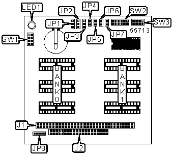
AAEON TECHNOLOGY, INC.
PCM-3810
| Card Type | Miscellaneous I/O Card |
| Maximum Onboard Memory | 2.88MB |
| Data Bus | PC/104 (16-bit) |

CONNECTIONS |
|||
Function |
Label |
Function |
Label |
| PC/104 connector (8-bit) | J1 | External battery connector | JP8 |
| PC/104 connector (16-bit) | J2 | ||
USER CONFIGURABLE SETTINGS |
|||
Function |
Label |
Position |
|
| » | Flash memory programming disabled (Bank 0) | JP1 | Pins 2 & 3 closed |
| Flash memory programming enabled (Bank 0) | JP1 | Pins 1 & 2 closed | |
| » | Flash memory programming disabled (Bank 1) | JP2 | Pins 2 & 3 closed |
| Flash memory programming disabled (Bank 1) | JP2 | Pins 1 & 2 closed | |
| » | External backup battery selected | JP3 | Pins 2 & 3 closed |
| Internal backup battery selected | JP3 | Pins 1 & 2 closed | |
| » | Factory configured - do not alter | JP4 | Unidentified |
| » | Factory configured - do not alter | JP5 | Unidentified |
| » | Master in two module system | JP6 | Closed |
| Slave in two module system | JP6 | Open | |
| » | Write protection disabled | JP7 | Closed |
| Write protection enabled | JP7 | Open` | |
| Backup battery enabled (Bank 0) | SW1 | Pins 1 & 2 closed | |
| Backup battery disabled (Bank 0) | SW1 | Pins 1 & 2 open | |
| Backup battery enabled (Bank 1) | SW3 | Pins 1 & 2 closed | |
| Backup battery disabled (Bank 1) | SW3 | Pins 1 & 2 open | |
DRAM CONFIGURATION |
||
Size |
Bank 0 |
Bank 1 |
120KB |
(1) 128KB x 8 |
None |
| 240KB | (1) 128KB x 8 | (1) 128KB x 8 |
| 240KB | (2) 128KB x 8 | None |
| 360KB | (3) 128KB x 8 | None |
| 360KB | (1) 512KB x 8 | None |
| 720KB | (3) 128KB x 8 | (3) 128KB x 8 |
| 720KB | (2) 512KB x 8 | None |
| 1.2MB | (3) 512KB x 8 | None |
| 2.88MB | (3) 512KB x 8 | (3) 512KB x 8 |
Note: Board supports SRAM/ROM/Flash memory types. |
||
MEMORY JUMPER CONFIGURATION (BANK 0) |
||||
| Type | SW1/Pins 3 & 4 | SW1/Pins 5 & 6 | SW1/Pins 7 & 8 | |
| » | SRAM 128KB x 8 | Open | Closed | Closed |
| ROM 128KB x 8 | Closed | Open | Closed | |
| Flash 128KB x 8 | Open | Open | Closed | |
| SRAM 512KB x 8 | Open | Closed | Open | |
| ROM 512KB x 8 | Closed | Open | Open | |
| Flash 512KB x 8 | Open | Open | Open | |
| Bank disabled | Closed | Closed | Closed | |
MEMORY JUMPER CONFIGURATION (BANK 1) |
||||
| Type | SW3/Pins 3 & 4 | SW3/Pins 5 & 6 | SW3/Pins 7 & 8 | |
| » | SRAM 128KB x 8 | Open | Closed | Closed |
| ROM 128KB x 8 | Closed | Open | Closed | |
| Flash 128KB x 8 | Open | Open | Closed | |
| SRAM 512KB x 8 | Open | Closed | Open | |
| ROM 512KB x 8 | Closed | Open | Open | |
| Flash 512KB x 8 | Open | Open | Open | |
| Bank disabled | Closed | Closed | Closed | |
| Note: If Bank 1 is enabled, then Bank 0 must also be enabled. | ||||
MEMORY ADDRESS SELECTION |
|||
Setting |
SW2/Pins 1 & 2 | SW2/Pins 3 & 4 | |
| » | D0000~D3FFF |
Closed | Open |
D4000~D7FFF |
Open | Closed | |
D8000~DBFFF |
Open | Open | |
Disabled |
Closed | Closed | |
I/O ADDRESS SELECTION |
|||
Setting |
SW2/Pins 5 & 6 | SW2/Pins 7 & 8 | |
22C~22D |
Closed | Closed | |
26C~26D |
Closed | Open | |
2AC~2AD |
Open | Closed | |
| » | 2DC~2DD |
Open | Open |
BANK DRIVE SELECTION |
|||||
Linked Mode |
Bank 0 | Bank 1 | SW2/Pins 9 & 10 | SW2/Pins 11 & 12 | |
| » | 1st |
1st | 2nd | Closed | Closed |
2nd |
3rd | 1st | Open | Closed | |
3rd |
1st | 3rd | Closed | Open | |
4th |
3rd | 4th | Open | Open | |
DIAGNOSTIC LED(S) |
|||
LED |
Color |
Status |
Condition |
| LED1 | Unidentified |
On |
Battey is low |
| LED1 | Unidentified |
Off |
Battery is normal |